|
||||||||||||||||||||||||||||||||||||||||||
|
||||||||||||||||||||||||||||||||||||||||||

Machine vision applications set imager choices
This is an article by Nixon O published by DALSA Corporation. ![]()
Much has been written about the relative advantages of CCD and CMOS technologies for image sensors. While such discussions are academically interesting, they reflect an us-versus-them approach more suited to promoting a given technology than to helping solve a machine vision design problem. Looking first at the application will allow developers to match each technology’s strengths to their needs.
The first application detail to consider is the type of image sensor needed. Image sensors for machine vision are typically one of two types: area sensors or line sensors. An area sensor is a two-dimensional array of pixels that captures an image of an entire region all at once, i.e., a snapshot. A line sensor is a one-dimensional, linear array of pixels that machine vision systems can use to build a 2-D image one line at a time.
There are also variations of the line sensor that are important enough to merit individual attention. One is the dual-line sensor that, as its name suggests, has two parallel linear arrays. Having the parallel pixel array gives the dual-line sensor added sensitivity.
The other important line sensor variant is the time delay and integration (TDI) sensor. This sensor has multiple linear arrays in parallel but is not an area sensor. Instead of exposing and transferring data from all the arrays simultaneously, the TDI sensor scans across the arrays. The timing of this scan coincides with the movement of an image segment across the array so that the signals from each array reflect the same image segment. The result is data that represent only a single line of the image, but are the accumulation of the information from all of the parallel arrays.
Choosing Sensor Type
The various sensor types address different applications. Area sensors are usable for most machine vision applications, but are required when the objects being studied are moving in two dimensions. Examples include security systems, where the scene may be stationary but the objects of interest (i.e., intruders) are moving throughout the scene, and robotic vision, where the system must control the 2-D movement of an arm. Area sensors are also used for making detailed inspections of a random area within a larger object.
Line sensors are most useful when the image subject is static, such as a document or other unchanging object. Machine vision systems can use line sensors to build 2-D images of static objects if either the object or the sensor is moving linearly. Examples include document scanning with a moving sensor and object scanning while the object is on a moving conveyor belt.
The dual-line sensor offers additional sensitivity in such applications. The information from the second line can be added to the first to double sensitivity. Dual-line sensors also offer exposure control for the image and can support sophisticated anti-blooming algorithms. For systems with high reliability requirements, the second array in the sensor provides redundancy.
TDI sensors are useful in situations where the light levels are low, creating a requirement for long exposures. By timing the transfers to occur at the same rate that the image moves across the arrays, each array captures the same image segment. Adding the data together essentially turns the TDI array into a line array with an effective exposure time equal to the sum of the exposure times for each line Using a TDI array in this manner, for example, allows line imaging where there is high-speed motion that would result in too short an exposure for a single line sensor.
Once the sensor type is chosen, a look at more specific application requirements is needed to establish which sensor technology makes the best choice. Some obvious parameters, such as pixel count, make little difference because both technologies can achieve similar pixel densities. Instead, operational details such as frame rate, low-light operation, and non-visible wavelengths become the key elements. For area sensors, functions such as electronic shuttering join frame rate as application requirements that technology choice can significantly impact.
Electronic Shuttering
Electronic shuttering is an ability to start and stop light collection in the sensor and is particularly important for CCD devices. As long as a CCD pixel is exposed to light it will accumulate charge, even during the time that the sensor is engaged in transferring its charge out to be read. As a result, if there is motion within the scene, the image that the sensor produces exhibits smearing.
The solution for CCD sensors is to create transfer channels, masked to block the light, adjacent to each line of image pixels (see Figure 1). This structure allows the sensor controller to use a single operation to transfer the entire image to the masked channels, stopping the exposure for that image, then shift out the image data without them accumulating any further charge. The penalty for using this interline transfer (ILT) structure is that the fraction of each pixel’s surface area that is light sensitive (fill area) is reduced, affecting overall sensor sensitivity. Still, most CCD area sensors for machine vision use the ILT structure. The use of microlenses on the sensor’s surface to concentrate incident light into the active region can help ameliorate, but not fully correct, the sensitivity loss, but can result in a response that varies with the angle of illumination.
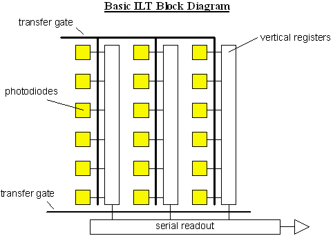
Figure 1: Masked inter-line transfer (ILT) channels provide electronic shuttering for CCD sensors, but reduce fill area.
With CMOS sensors, electronic shuttering is accomplished through the use of transistors in each pixel to control the connection between the light-sensing photodiode and the charge storage capacitor. Because these transistors are light blocking, they reduce the pixel fill area. To maximize fill area, some CMOS area sensors use a 3-transistor pixel structure that ends up providing a “rolling shutter,” affecting exposure for one line of the image at a time. This rolling shutter can distort the final image (See Figure 2) if the subject is moving. Achieving a true global shutter that provides an arbitrary exposure time requires a 5-transistor pixel structure, with resultant loss of fill area and sensor sensitivity. As with CCD sensors, microlenses can improve sensitivity.
a)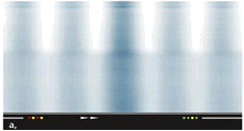 b)
b)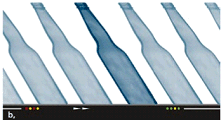 c)
c)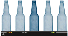
Figure 2: Without electronic shuttering images may blur(a) with motion. The rolling shutter effect of a 3-transistor CMOS pixel design can result in image distortion(b) when objects are moving. Global shuttering is needed to freeze motion without distortion(c).
Frame Rate
A second application requirement for area sensors that technology choice affects is the frame rate. For CCD sensors, the speed of delivery for pixel data sets the upper limit for frame rate. This limit arises because a CCD sensor must transfer out all of its pixel information in order to empty its transfer registers so that they can accept the next image. For a given pixel rate, then, the larger the image the lower the frame rate. The same holds true for linear sensors, but the tradeoff is less.
In practice, the upper limit on CCD pixel rate stems from the amplifier bandwidth at the charge-to-voltage conversion stage. Faster pixel rates require greater amplifier bandwidth, but greater bandwidth also brings in more noise. Further, high-speed, wide-band amplifiers are power hungry. Ultimately, then, frame rate of a CCD sensor involves a tradeoff among pixel count, noise, and power considerations.
An architectural trick can yield increased frame rates for CCD sensors: break the image into segments and provide amplifiers for each segment. Segmenting the image in this way and reading out the segments in parallel achieves a given frame rate with lower pixel rates at the amplifiers. For some applications, however, this approach is impractical because of the cost and the additional board space and power that the extra amplifiers would require.
Because CMOS sensors convert charge to voltage at each pixel, the amplifiers do not need to be high speed in order to support a fast frame rate. Thus, CMOS sensors can achieve faster frame rates more easily than CCD sensors. Further, unlike CCDs, the image data of CMOS sensors can be cleared without having to be read. This allows the machine vision system to read out only a portion of the image information, working with an area of interest within the image. By reading out only the area of interest, CMOS sensors can support a faster frame rate without increasing the pixel rate.
Low-light Operation
When an application requires low-light operation, differences in CCD and CMOS technology impact image quality. At low light levels, where amplifier variations are more significant, CCD sensors have more uniform pixel response than CMOS sensors. The individual charge-to-voltage amplifiers at each CMOS pixel have gain and offset values that are difficult to match. Further, they are not adjustable. CCD sensors use the same amplifier for all the pixel data from a given output, so pixel variation is less.
Low light conditions mean that the resulting signals are close to the sensor’s noise floor. Because the individual amplifiers for CMOS pixels have low bandwidth, they have lower noise than the high-bandwidth, common CCD amplifier. This allows the amplifier to offer higher gain before noise levels become intolerable, yielding a higher effective signal-to-noise (S/N) ratio for CMOS sensors. On the other hand, CCD sensors typically offer better fill areas, so the pixels are more sensitive and provide greater signal levels at low light. Further, CCD sensors can use a technique called electron multiplication, which imparts a small signal gain each time the pixel charge transfers to the next stage of the output shift register. While noise also increases with each transfer, it increases at a lower rate so the result of electron multiplication is an improvement in S/N ratio.
There is also a method of operation that can increase the sensitivity of CCD sensors: binning. When binning, a CCD sensor transfers charge from one pixel to an adjacent pixel, combining the two charges. This combination cuts the effective resolution in half but effectively doubles pixel sensitivity. Because binning in CCD sensors involves the addition of charges, no noise gets added to the signal when signals are combined. Binning together N pixels gives an N-fold improvement in S/N ratio.
The operation equivalent to binning in CMOS sensors, however, requires sampling the voltage signals from adjacent pixels then adding the results together. The sampling step inserts some random noise into the signal. Adding together the pixel values, then, adds together these random noise contributions. As a result, binning N pixels in a CMOS sensor yields only a N increase in S/N ratio.
Other Wavelengths
Differences in CCD and CMOS technologies are also significant when using light sources outside of the visible spectrum. Long-wavelength light such as infrared (IR), for instance, penetrates deeper into the silicon than visible light before being absorbed. Thus, in order to have adequate sensitivity, a pixel’s active region must also be deeper. Fabricating a deep pixel structure is relatively easy in CCD technology, but is problematic in CMOS technology. A deep structure in a CMOS pixel means that all the other transistors in the device must also have a deeper substrate, adversely affecting the performance of control transistors, amplifiers, multiplexers, and the like.
Working with ultraviolet (UV) light sources is equally problematic. Most of the layers of an integrated circuit are either not completely transparent to UV or are affected by UV. As a result, the signals that the active pixel regions produce can be weak when illuminated from the sensor’s top surface. The solution to this masking effect of the sensor’s top layers is to make the device thin by removing substrate material and illuminating the sensor from the back surface. The fabrication processes for thinning CCD sensors are mature and well controlled, but the processes for thinning CMOS sensors are still under development (Ref 1.)
The technology differences of CCD and CMOS sensors as they affect electronic shuttering, frame rate, low-light operation, and non-visible wavelength illumination show that the technology choice for an area sensor strongly depends on the relative importance of these application needs. For applications needing low-light or non-visible wavelength operation, the advantages of CCD technology make it the better choice. For applications where higher frame rates and lower power are most important, or where the application needs to be able to concentrate on an arbitrary area of interest, CMOS technology gives better results. If electronic shuttering is a prime requirement, the two technologies simply imply different tradeoffs.
Line Sensor Tradeoffs
Many of these same technology differences apply when using line-scan sensors, although a few of them become less important. The sensor’s speed, for example, is less of an issue because there are fewer pixels involved. Similarly, the differences in fill area disappear even when electronic shuttering is required. The additional transistors that reduce fill factor for a CMOS area sensor can be placed alongside the pixel array, outside of the active area, in a line sensor.
There are application considerations that rise in importance with line sensors, however. One is color operation. For a sensor to produce a color image it needs three arrays, one each for red, green, and blue components of the image (see Figure 3). Because a CCD sensor needs transfer and readout circuits adjacent to its pixels, the three color arrays are spaced apart. A CMOS line sensor, on the other hand, can position its circuitry at a distance from the pixel arrays, allowing the pixels to be positioned more closely together. This closer spacing improves image resolution and helps minimize motion-generated image artifacts.
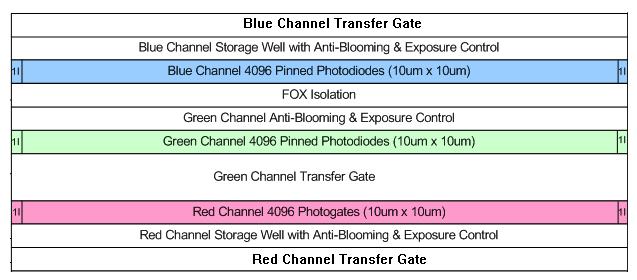
Figure 3: Because it needs transfer and readout circuitry next to each pixel, a CCD sensor for color images ends up sacrificing resolution in order to provide parallel arrays for each primary color.
Still, unless color operation is required, simple line scan sensors do not demonstrate as significant a technology difference as is seen with area sensors. The most distinguishing feature of the technologies is their relative maturity. Because CCD sensors have a longer history, the challenges and solutions for their use in machine vision applications are better understood.
For TDI line scan sensors, however, technology differences become more significant. These sensors target a specific type of application where the image is formed through the steady, linear movement of an object across the sensor’s field of view (see Figure 4). The output signal of a TDI sensor is the result of binning together as many as 100+ linear pixel arrays, so the binning considerations of sensor technology become paramount. Because CCD sensors add pixel data together without added noise, they achieve an N-fold increase in S/N ratio with N lines, while CMOS sensors add pixel data with noise, yielding a N increase in S/N ratio. With a 100-line TDI design, CCD sensors thus have 10x the S/N ratio of an equivalent CMOS sensor, giving the CCD sensor a much greater dynamic range.
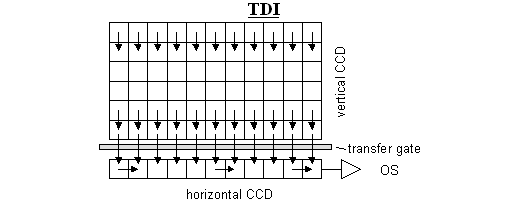
Figure 4: A TDI sensor coordinates its data transfers to match an object’s motion, effectively turning the entire array into a highly-sensitive line sensor.
Begin with the Application
It is clear, then, that making a machine vision sensor selection should begin not with the fabrication technology, but with the application. Developers should first determine whether an area sensor, a line sensor, or a TDI sensor is the best fit for their imaging needs. Once the sensor type is selected, developers should then determine their requirements for frame rate or imaging speed, the light sensitivity and dynamic range they will need, and whether or not to use color imaging or non-visible light for illumination. By prioritizing these requirements, a comparison of technologies will then show the relative strengths of CCD and CMOS technology in the given application.
It should be noted, however, that these relative strengths are continually changing as each technology evolves. Among CMOS image sensors, for instance, vendors are concentrating on increasing sensor pixel counts and transfer speeds to achieve higher frame rates. Improvements in CCD sensors include increased sensitivity through electron multiplication and improved sensitivity through the creation of dual-line sensors.
In the face of these changing technologies, developers are best served by working with companies such as Dalsa that focus on providing solutions rather than selling specific technologies. With area sensors, for instance, Dalsa offers both CCD and CMOS sensors and DALSA’s machine vision segment is concentrating its development efforts on CMOS technology to further increase its speed advantages. In line sensors, Dalsa is committed to providing the best sensor for an application whichever technology is involved.
By looking first at their application needs, developers can avoid getting mired in trying to evaluate the complex and subtle differences between CCD and CMOS image sensor technologies. Having insight into the attributes that are significant to their project and knowing the relative importance of those attributes can go a long way toward making the right technology selection. With the support of companies like Dalsa that impartially offer both CCD and CMOS sensors, the final steps in sensor selection are easy to make.
About the author
Nixon O is the Technical Director responsible for the development of technology roadmaps for DALSA’s machine vision products. His areas of expertise include image sensors, semiconductor fabrication processes and integrated circuit design. Nixon holds a PhD in Electrical Engineering from the University of Waterloo (Waterloo, Ontario), the topic of his thesis is ‘CCDs for non-optical sensing.’ He is an active member of the Institute of Electrical and Electronics Engineers (IEEE). He has over 16 years of experience in CCDs and image sensors and has played a pivotal role in the early development of DALSA’s Linescan, TDI sensor and camera technologies.
Adept Electronic Solution (AES) is the exclusive distributor of Dalsa products to Australia and New Zealand. To find out more about this article or Dalsa products please email us at: adept@adept.net.au or call us at Perth (08) 92425411 / Sydney (02) 99792599 / Melbourne (03) 95555621.
For more information please contact us.
|
If you like this page, please recommend and share it. |
||
| More | ||