|
||||||||||||||||||||||||||||||||||||||||||
|
||||||||||||||||||||||||||||||||||||||||||

Sensor Comparison II: Interline Scan, Frame Transfer & Full Frame
Last month our feature article discussed the differences, pros and cons of Interlaced Scan and Progressive Scan sensors. If you missed it, or would like a refresher, click here. This month we are discussing the Interline Transfer architecture for CCD’s and how it compares to that of Frame Transfer and Full Frame sensors. Almost all CCD industrial cameras available these days use Interline Transfer sensors. Some cameras however use Frame Transfer sensors because of their specific advantages in some applications. There are few if any Full Frame sensors used in modern industrial cameras because they lack significant advantages over Frame Transfer. The key difference between Interline transfer, Frame Transfer and Full Frame sensors is where the pixel charge is stored after it is acquired and during the next integration period while the current image is being read out of the sensor. To explain it is first best to describe the sensor image capture process in more detail:
The difference between Interline transfer, Frame Transfer and Full Frame sensors is where the electrons (pixel charge) are stored (if stored) before being read out of the sensor.
Interline Transfer CCDIn Interline transfer CCD sensors each and every pixel has a charge storage area next to it. The charge storage area of each pixel is masked so that photons cannot hit it. The pixel storage areas form a vertical column to the bottom of the sensor. This vertical column is used to transport the pixel charges down and out the bottom of the sensor. The light sensitive pixel area (active area) is electrically separated from the storage pixel area and so the active pixel area can act independently of the storage area. At the end of the integration period the charge in every active pixel is shifted to its adjacent pixel storage area. At this point the active pixel area is reset and the next integration period starts while the charges in the storage pixels are clocked down to the bottom of the sensor. This is analogous to a bucket brigade where you have a row of buckets full of water (electrons) where the last bucket empties its contents before it is filled by the water from the bucket before it, and when the bucket before it is empty it in turn is filled by the water in the bucket before that and so on. This happens with all pixels on a line simultaneously so that lines of pixel charges are clocked down together. This in fact is where a CCD gets its name from - Charge Coupled Device - charges are coupled pixel by pixel and transported out of the sensor. When a pixel charge reaches the bottom of the sensor it is clocked down once more to a shift register. The pixel charges in the shift register at any one point in time represent the pixels acquired on a row of the sensor during the earlier integration period. Once the pixel charges are in the shift register they are clocked out at a rapid rate before the next row of pixel charges is clocked into the shift register. From the shift register the pixel charges are fed to amplifiers which convert charge to voltage. The voltage is then conditioned further, digitised in the case of digital cameras and then fed out the back of the camera. The key advantage of Interline Transfer CCDs is that the charge from an integration period can very quickly be shifted to the storage pixel area. This allows the active pixels to be reset and to acquire the next image in the next integration period while the pixel charges from the previous image are being clocked down the storage pixel columns and out the sensor via the shift register. So both image acquisition and readout is happening in parallel which facilitates faster frame rates. Interline Transfer CCD sensors avoid (minimise) image smear by the fact that the pixel storage area is masked so light cannot hit it. If they were not covered then photons hitting the storage area while a charge is being clocked down through that storage area, would have electrons added to it. This has an effect in an image that looks like and is called smear. If the image scene has a bright point, this bright point would be smeared vertically down the image. Another advantage of Interline Transfer CCD sensors is that the sensor area is relatively small and so relatively inexpensive to manufacture. There is however a cost to covering up half the pixel area for storage. It reduces the area of each pixel available to collect light (this is called Fill Factor) and so is less sensitive. Interline Transfer is therefore not the best sensor technology to use for applications that are starved for light however are very good in many or most other applications. Some Interline Transfer sensors are fitted with micro-lenses covering every pixel which direct light away from the masked storage area of each pixel onto the active area. These sensors are called HAD or Hyper HAD and have significantly higher effective Fill factor as compared to Interline sensors without micro-lenses. The Jai CVM4+CL is an example of a camera with hyper HAD sensor and is often used for light starved situations such as night time intelligent traffic applications. There two different types of Interline Transfer sensors: Interline Transfer - Interlaced Interline Transfer - Progressive Scan
|
|
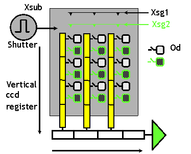
Interline Transfer CCD - InterlacedThe Interlaced version of the Interline Transfer CCD sensor consists of a pixel array for each field. The pixel from each field is connected through the Xsg switch to a storage pixel area in the vertical CCD. From here the collected charge is shifted to the horizontal CCD and read out line by line as a video signal. With frame integration the charge from field 1 is transferred to the vertical CCD by Xsg1 and read out as first field. Then the charge from field 2 is read out as field 2. The result is an interlaced frame. In field integration the charge from both fields are read out and added in one vertical CCD cell. The result is a 2 to 1 vertical binning so only half the vertical resolution is obtained. The shutter (reset and integration) function operates by draining all pixels from both fields in parallel with Xsub until the wanted exposure time before the Xsg pulse. It is seen that only a single field can be the result of a single shutter event.
|
 |
Interline Transfer CCD - Progressive Scan |
||
|
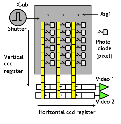
The CCD sensor consists of a pixel array for the full frame. Each pixel is connected through the Xsg switch to a storage pixel area in the vertical CCD. From here the collected charge can be shifted to either one ore two horizontal CCD registers. With one vertical shift per line the frame is available as a progressive scanned frame from video 1 output. Some sensors allow for two outputs and so with two vertical shifts per line a field is available from the two video outputs. The two outputs are then combined in a frame grabber to a full progressive frame image. The frame rate is double that from a single output. A full frame can be the result of a single shutter event.
|
|
Frame Transfer CCDFrame Transfer CCDs are inherently progressive scan. They capture a full frame in a single shutter (integration) period. They differ from Interline Transfer CCDs because they do not have a pixel storage area next to the active pixel and instead have a duplicate sensor used for storage below the active sensor. So for example a 640x480 pixel Frame Transfer sensor has a 640x480 active pixel array above another 640x480 storage pixel array. The storage pixels are masked (covered) so that no photons can hit them. The image capture process for a Frame Transfer sensor begins with the integration period where the active pixels collect electrons that are converted from photons. At the end of the integration (shutter) period the 480 lines (using the example above) of active pixels (640 pixels per line) are clocked down line by line (as fast as possible) until all 640x480 pixel charges are stored in the 640x480 storage pixel array. The time it takes to clock all 480 lines from the active pixel area to the storage pixel area is called the Readout Time. When the Readout has been completed the active pixels are reset and begin the next integration period while the pixel charges in the storage area are clocked out line by line to the shift register. From the shift register they are in turn clocked out the back of the camera via amplification and conditioning circuitry as happens with Interline Transfer sensors. The benefit of Frame Transfer sensors is that since they do not share active pixel area with storage pixel area they have 100% Fill Factor and so all of the active pixel area is used to accept photons. This makes Frame Transfer sensors very sensitive and is generally the main reason they are used. The disadvantage of Frame Transfer sensors is that while the active pixel charges are being clocked down to the storage pixel area during the Readout Time, they are not covered and so any light hitting the active pixel area adds to each pixel charge as it passes through. A bright spot in the image therefore causes smear. The general rule of thumb is that if the shutter time is less than ten times longer than the Readout Time then the smear is significant and should be addressed. One way to eliminate smear is to use a mechanical shutter on the camera that blocks light to the active pixel area at all times other than during the integration period. Another method is to use a bright strobe light synchronised to the shutter time. An example of a camera using a Frame Transfer sensor is the Dalsa Pantera 1M30. It features 1024x1024 pixels, with 100% Fill Factor and large 12x12um pixel area. It offers excellent 40DN/nj/cm2 responsivity and a very high 66dB dynamic range.
Full Frame CCDFull Frame CCDs are inherently progressive scan. They capture a full frame in a single shutter (integration) period. They differ from Interline Transfer CCDs because they do not have a pixel storage area next to the active pixel. They in fact have no pixel storage area. The image capture process for a Full Frame sensor begins with the integration period where the active pixels collect electrons that are converted from photons. At the end of the integration (shutter) period the 480 lines (using the example above) of active pixels (640 pixels per line) are clocked down line by line to the shift register to be clocked out the back of the camera via amplification and conditioning circuitry as happens with Interline Transfer sensors. The benefit of Full Frame sensors is that they have 100% Fill Factor and since they require half as much pixel area as Frame Transfer sensors they are less expensive. The disadvantage of Full Frame sensors is that it takes a relatively long time to clock the pixels out of the shift register and so the effective Readout Time is long and so they suffer smear badly. Full Frame sensors are always used with a mechanical shutter or strobe light. It seems that very few industrial manufacturers use Full Frame sensors these days and if you find them at all it will be in a specialist scientific camera.
Adept Electronic Solutions are 'The Machine Vision and Imaging Specialists' in Australia and New Zealand. To find out more about sensor types or information on machine vision please email us at: adept@adept.net.au, call us at Perth (08) 92425411 / Sydney (02) 99792599 / Melbourne (03) 95555621 or use our online contact us form. |
|
If you like this page, please recommend and share it. |
||
| More | ||